AI · SEMICONDUCTOR · FACT CHECK
 SKD WIRE
True
Applied Materials and BE Semiconductor Industries (Besi) have expanded their strategic partnership targeting the next-generation semiconductor packaging market, deepening collaboration on advanced packaging equipment and technologies as demand grows for AI-driven chip architectures.
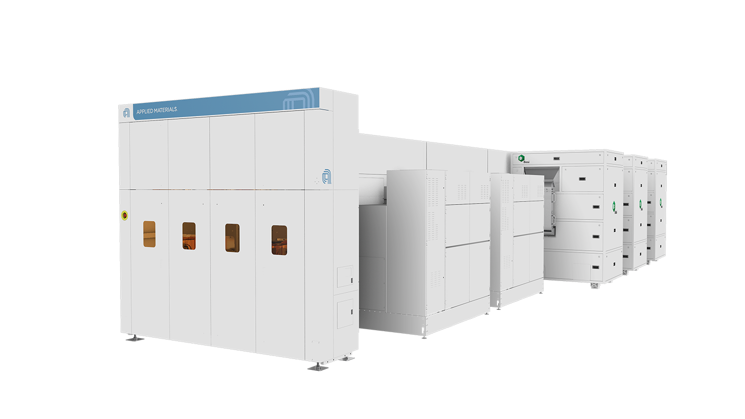
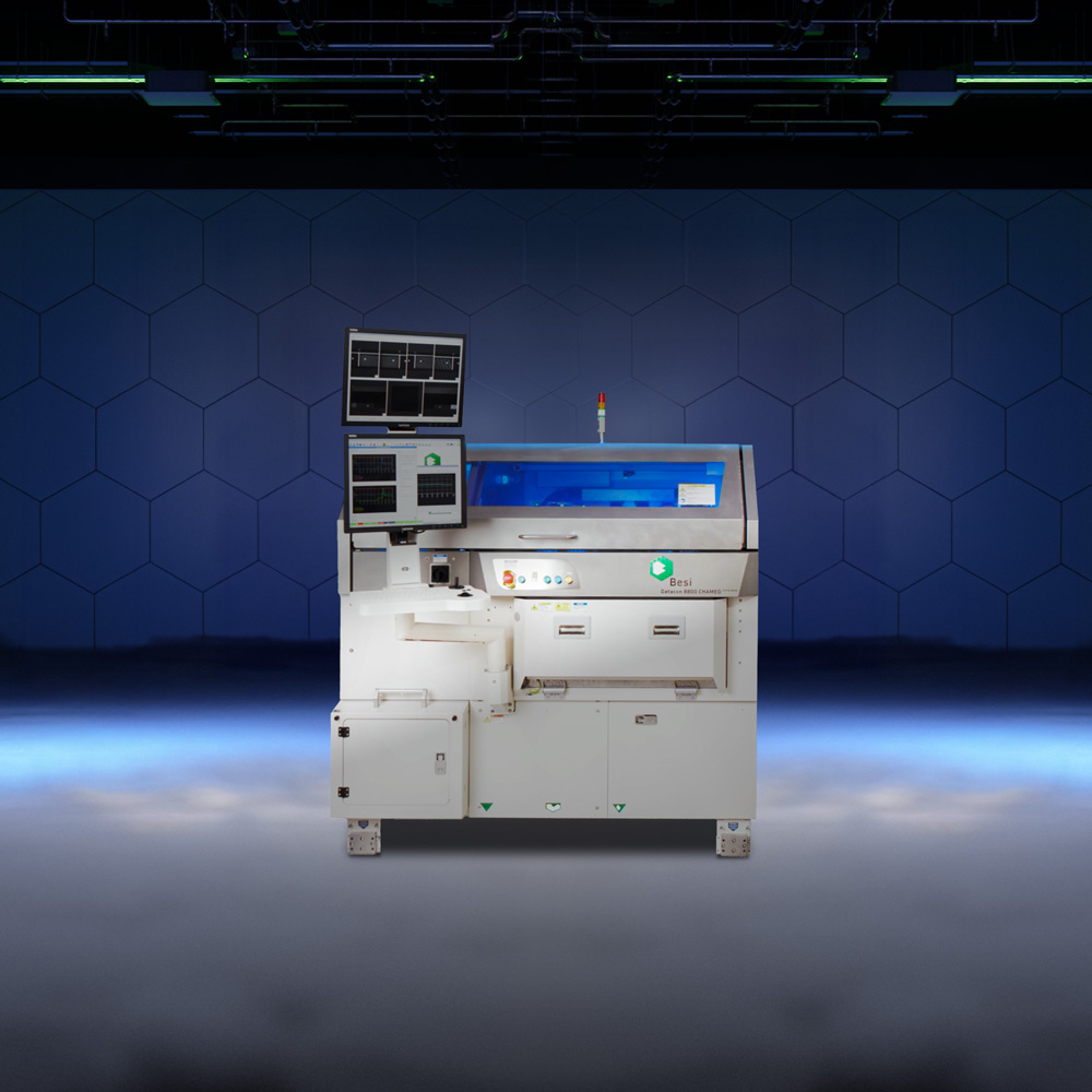
The collaboration between the two equipment makers centers on next-generation packaging — a field that has become increasingly critical as chipmakers seek to overcome the limits of traditional transistor scaling. Applied Materials brings its process equipment portfolio, including technologies associated with its Kinex platform, while Besi contributes its die-attach and hybrid bonding expertise, represented by products such as the Datacon 8800 CHAMEO ultra plus AC.
The partnership reflects a broader industry shift in which advanced packaging — combining multiple chips and dies into high-performance modules — has become a key battleground for equipment suppliers as AI workloads drive demand for high-bandwidth memory and complex heterogeneous integration.
Next-generation packaging has moved from a niche segment to a strategic priority for semiconductor manufacturers worldwide, with companies investing heavily in capabilities that support the assembly of advanced AI accelerators and high-performance computing devices. Equipment suppliers capable of delivering integrated solutions for these processes are positioning themselves accordingly.
Details such as the financial terms of the expanded partnership and its specific customer engagements were not provided in the announcement.
The claim that Applied Materials and Besi have expanded their strategic partnership in the next-generation packaging market is True.