AI · SEMICONDUCTOR · FACT CHECK
 SKD WIRE
Mostly True
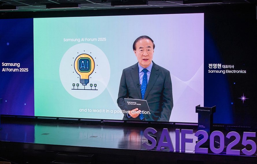
Samsung Electronics is targeting a reduction of up to three years in the development cycle for new semiconductor materials by applying AI across its materials research process, according to statements and materials from the company's official channels and related symposium coverage.
The company has been pursuing AI-driven techniques to accelerate the discovery and validation of new semiconductor materials, a process that traditionally takes a long time from initial research to mass-production readiness. The three-year reduction is presented as a goal rather than a completed achievement.
The claim traces to Samsung's official communications, including its material and core technology announcements, though direct access to one official Samsung page was delayed during research and confirmation was made via the company's alternative official channel, the Samsung Semiconductor Newsroom. Details of a related symposium — identified in coverage as a KIAF symposium — could not be fully obtained.
The three-year figure should be understood as a development target announced by the company, not an independently measured outcome. Uncertainty remains around the precise scope of the claim, including which material categories and process stages the reduction applies to, and the full details of the symposium presentation were not available.
The core assertion — that Samsung Electronics has set a goal of shortening new semiconductor material development by three years through AI — is supported by the company's official materials. On that basis, the claim is assessed as Mostly True.
