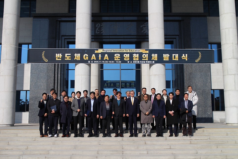
Hanyang University ERICA to strengthen industry-academia-research GAIA hub through shared semiconductor FAB
Mostly True

Hanyang University ERICA is moving to build a shared semiconductor FAB, a step intended to reinforce its role as a GAIA hub for industry-academia-research collaboration. The project would give the campus-based hub dedicated fabrication infrastructure to support joint research and talent development in the semiconductor field.
Shared FAB as the core of the GAIA hub strategy
The plan centers on establishing a semiconductor shared FAB on the ERICA campus in Ansan. Such a facility would allow companies, research institutes, and the university to jointly use fabrication and testing capabilities, lowering the entry barrier for fabless and foundry-related work in the region.
The GAIA initiative, led by the Ministry of Science and ICT, designates regional bases for AI research and industry cooperation. Hanyang University ERICA serves as one such hub, and the shared FAB is positioned as a way to deepen its semiconductor capabilities alongside its AI focus.
Uncertainty over timeline and scope
Details such as the facility's exact scale, investment size, and construction schedule have not been made fully public, and the project remains at a stage where specifics could change. What is established is the direction: the shared FAB is intended as infrastructure for joint use by the university and its industry and research partners.
The initiative aligns with broader national efforts to strengthen the domestic semiconductor ecosystem, particularly in supporting smaller fabless firms that lack access to fabrication facilities of their own.
Hanyang University ERICA's push for a shared semiconductor FAB to reinforce its GAIA hub role is supported by the core facts of the plan, though key details on scale and timing remain open — making the claim Mostly True.
- https://news.unn.net/news/articleView.html?idxno=597827
- https://ericarise.hanyang.ac.kr/front/ko/union/semicenter
- https://news.unn.net/news/articleView.html?idxno=597969
- https://blog.naver.com/PostView.naver?blogId=hyerica4473&logNo=224095549994
- https://blog.naver.com/PostView.naver?blogId=hyerica4473&logNo=224245333990
- https://www.news1.kr/society/education/5807455
- https://www.google.com/search?q=…
- https://html.duckduckgo.com/html/?q=…
- https://ericarise.hanyang.ac.kr/resources/front/images/subpage/union/semicenter/img-1.png
- https://postfiles.pstatic.net/MjAyNTEyMDJfMjU0/MDAxNzY0NjU0MjAzNzIy.yuNhF0VAgvnYBMoQXo6utuTULlnhyk4Txg-6_5yoJzcg.NWG7NuB5JyXyd_UrxBVzuy27Esxf-VzOO7DWTtzz7N8g.JPEG/IMG_0726.JPG?type=w966
- https://cdn.news.unn.net/news/photo/202609/597827_423807_4320.png**