AI · SEMICONDUCTOR · FACT CHECK
 SKD WIRE
Mostly True
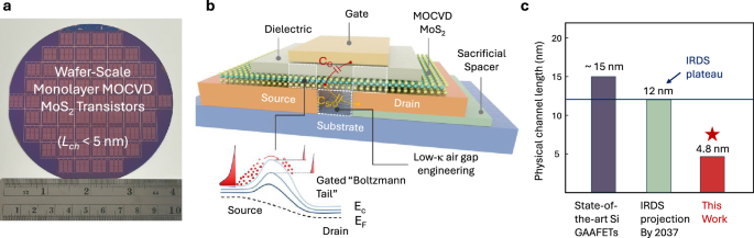
A claim that two-dimensional (2D) materials could help semiconductors overcome the physical limits of silicon holds up as broadly accurate, according to a review of primary sources including a Gwangju Institute of Science and Technology (GIST) announcement and a peer-reviewed paper published in Nature Communications.
The claim, reported in Korean as "2D materials to cross the silicon limit," asserts that atomically thin 2D materials are being positioned as a successor path as silicon-based semiconductor scaling approaches its physical limits. The research summary records the final assessment of the claim as "mostly true."
The underlying work is documented in a Nature Communications paper, with figures published alongside the article by Springer Nature. GIST, whose release is linked among the primary sources, is associated with the research. The publication of the findings in a peer-reviewed journal supports the core of the claim that 2D materials are an active research direction for post-silicon electronics.
While the claim's general thrust is supported, the record does not establish that 2D materials have reached commercial readiness or that they will definitively replace silicon in mass production. As with much early-stage materials research, the transition from laboratory demonstration to volume manufacturing remains a significant hurdle, and the reviewed sources do not confirm a timeline for such a shift.
The claim that 2D materials are being pursued as a way to go beyond the limits of silicon is broadly supported by the available evidence, though the extent of their practical impact is not yet settled — the finding is best described as Mostly True.