AI · SEMICONDUCTOR · FACT CHECK
 SKD WIRE
True
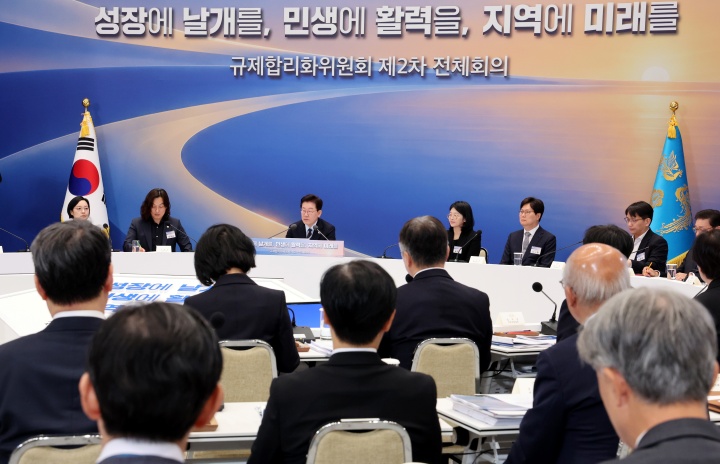
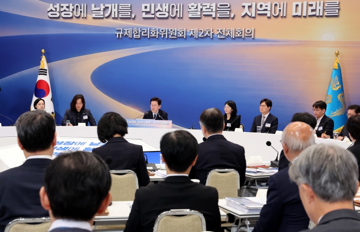
The South Korean government is moving to advance permitting, compensation and design phases of a semiconductor industrial complex concurrently, rather than sequentially, in an effort to shorten the timeline for bringing new chip manufacturing sites online.
Under the approach, administrative steps that traditionally follow one another — licensing and permits, compensation for landowners, and site design — are to be pursued at the same time. The structure is intended to reduce the multi-year lead times that have historically slowed the development of large-scale semiconductor manufacturing complexes in Korea.
The finding is documented in a verification report dated October 23, 2026, which examined the government's simultaneous-track approach to the semiconductor industrial complex (reports/2026-10-23_반도체산단_인허가보상설계_동시추진_검증보고서.md).
Accelerated site development carries direct relevance for Korea's leading semiconductor manufacturers, including Samsung Electronics and SK hynix, both of which depend on timely availability of industrial land for fabs and related infrastructure. Faster permitting and compensation could shorten the period between a site's designation and the start of construction.
Details on specific sites, budgets or schedules were not included in the material reviewed, and the extent to which concurrent processing changes statutory review requirements remains to be seen.
The claim that the government is advancing permits, compensation and design in parallel is True.