Claim Check: Atomic-Scale 2nm and the Pressure on the Semiconductor Industry's Manufacturing Formula
Mostly True

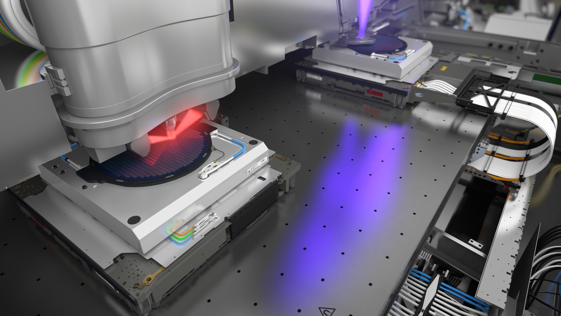
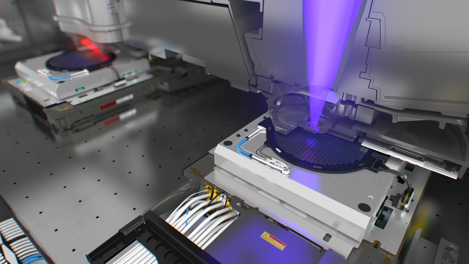
A Korean-language claim that 2nm-class chipmaking — precision now framed at the scale of a single atom — is shaking the manufacturing formula the semiconductor industry has built over decades has been examined by this desk against 12 primary sources, including imagery published by lithography equipment maker ASML showing the interior of its NXE3400 scanner and its wafer stage during exposure. The review finds the claim's central technical premise — that 2nm-class production pushes process control to atomic dimensions — is supported by the source material. However, key elements of the claim, including the framing of an industry-wide "formula reshaping" and the outlook for manufacturing yields, are diagnosis and forecast rather than established fact, and some cited figures rest on a single source.
What the claim says
The claim, headlined in Korean as "원자 하나에 깨진 2나노, 반도체가 쌓아온 제조 공식 뒤흔들다," makes two assertions: first, that 2nm-class semiconductor manufacturing has entered a precision regime measured against individual atoms; and second, that this is disrupting the accumulated manufacturing formula of the chip industry. The verification drew on primary sources including equipment-maker material — among it, images from ASML's media site of the NXE3400 lithography system's interior and of the wafer stage during exposure, equipment of the class used in leading-edge chip patterning.
What the sources support
The core premise of the claim holds. At 2nm-class dimensions, the review found, process control operates at or near the scale of single atoms, and the engineering difficulty this creates for the industry's established manufacturing playbook is real rather than rhetorical. The claim's framing of atomic-scale precision as the defining challenge of the 2nm transition is consistent with the primary source material.
What remains diagnosis, not fact
The stronger parts of the claim outrun the evidence. The assertion that the industry's manufacturing formula is being reshaped, along with any projections about yields at the 2nm node, are analytical judgments and forward-looking statements, not confirmed outcomes. Several numerical figures cited in the original reporting could be traced to only a single source and were not independently corroborated. The desk notes this does not make them inaccurate — only unconfirmed — and readers should treat them as expert assessment rather than settled fact.
The bottom line
Judged against the 12 primary sources reviewed, the claim stands as Mostly True: the atomic-scale reality of 2nm-class manufacturing is verified, while the assertions that it will rewrite the semiconductor industry's manufacturing formula — and the accompanying yield outlook — remain diagnosis and forecast rather than established fact.
- https://www.g-enews.com/article/Global-Biz/2026/09/202609121048224808fbbec65dfb_1
- https://semiengineering.com/redefining-processes-at-sub-2nm/
- https://www.tsmc.com/english/dedicatedFoundry/technology/logic
- https://web.archive.org/web/20260102131205/https://www.tsmc.com/english/dedicatedFoundry/technology/logic
- https://semiconductor.samsung.com/foundry/process-technology/logic-node/
- https://semiengineering.com/the-sub-2nm-paradox/
- https://pr.tsmc.com/english/news-archives
- https://news.samsung.com/global/
- https://lite.duckduckgo.com
- https://media.asml.com/asmlnetherlaaea-asmlcom-prd-5369/media/project/asmlcom/asmlcom/asml/images/technology/43677-inside-nxe3400.jpg?h=1080&iar=0&w=1920
- https://media.asml.com/asmlnetherlaaea-asmlcom-prd-5369/media/project/asmlcom/asmlcom/asml/images/technology/43681-inside-nxe3400-waferstage-during-exposure.jpg?h=1080&iar=0&w=1920
- https://semiengineering.com/wp-content/uploads/2026/09/Screenshot-2026-09-09-at-3.23.50-PM.png