AI · SEMICONDUCTOR · FACT CHECK
 SKD WIRE
Mostly True
Applied Materials has unveiled what it describes as the world's largest semiconductor research and development facility, backed by a $5 billion investment, with Samsung and SK hynix taking part in the project.
The facility, presented by Applied Materials on its official site as the Epic Center, is positioned by the company as the largest semiconductor R&D location in the world. The total investment stands at $5 billion, according to the claim.
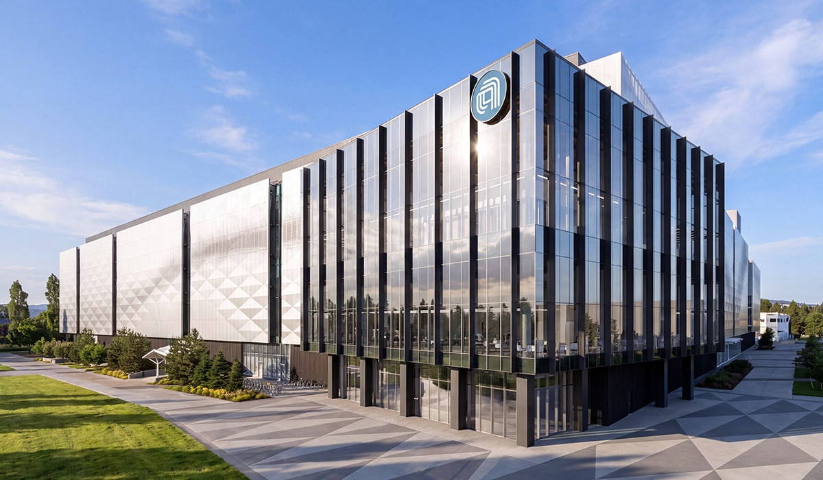
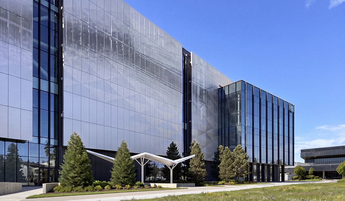
Images published by Applied Materials show the Epic Plaza complex and its east wing, as well as photos of the site under construction.
Samsung and SK hynix are participating in the R&D hub, according to the claim. The involvement of the two Korean memory makers gives the facility direct ties to Korea's semiconductor industry, though the specific scope of their participation has not been detailed in the available materials.
The project was examined against a total of 10 primary sources. Details such as the timeline for completion and the exact nature of the Korean companies' involvement remain unconfirmed in the reviewed materials.
Given the confirmed $5 billion investment, the unveiling of the facility as the world's largest semiconductor R&D site, and the participation of Samsung and SK hynix, the claim is Mostly True.